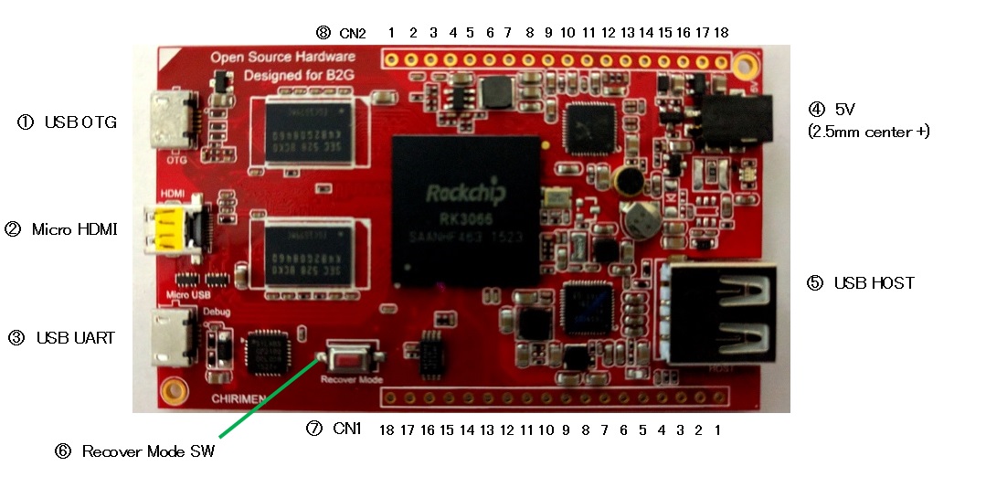
This section introduces the layout of connectors and switch of a CHIRIMEN board computer.
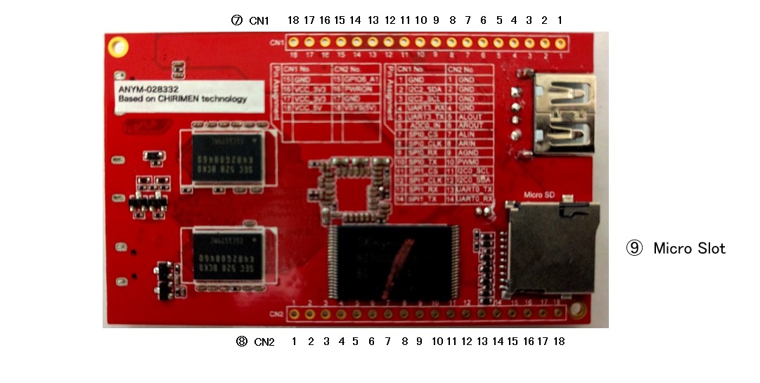
Multiuse I/O (CN1 and CN2) is
If you have not soldered any pins onto a CHIRIMEN yet, a jumper wire for Through Hole (e.g. TTW-200 ) is recommended for test use.
Note: Currently UART, SPI and PWM are re-assigned to GPIO.
| CN1 (Connector1) | |||
|---|---|---|---|
| Number | Description (sysfs name) | Drive | Pull up/down |
| 1 | GND | N/A | N/A |
| 2 | I2C-2 SDA | 8mA | UP |
| 3 | I2C-2 SCL | 8mA | UP |
| 4 | GPIO-3 D3 (gpio283) | 8mA | UP |
| 5 | GPIO-3 D4 (gpio284) | 8mA | DOWN |
| 6 | ADC-0 in | N/A | N/A |
| 7 | GPIO-1 A4 (gpio196) | 8mA | UP |
| 8 | GPIO-1 A5 (gpio197) | 8mA | DOWN |
| 9 | GPIO-1 A6 (gpio198) | 8mA | UP |
| 10 | GPIO-1 A7 (gpio199) | 8mA | UP |
| 11 | GPIO-1 C4 (gpio244) | 8mA | DOWN |
| 12 | GPIO-1 C3 (gpio243) | 4mA | DOWN |
| 13 | GPIO-1 C6 (gpio246) | 8mA | DOWN |
| 14 | GPIO-1 C5 (gpio245) | 8mA | DOWN |
| 15 | GND | N/A | N/A |
| 16 | VCC 3.3V | N/A | N/A |
| 17 | VCC 3.3V | N/A | N/A |
| 18 | VCC 5V | N/A | N/A |
| CN2 (Connector2) | |||
|---|---|---|---|
| Number | Description (sysfs name) | Drive | Pull up/down |
| 1 | GND | N/A | N/A |
| 2 | GND | N/A | N/A |
| 3 | GND | N/A | N/A |
| 4 | GND | N/A | N/A |
| 5 | Audio L out | N/A | N/A |
| 6 | Audio R out | N/A | N/A |
| 7 | Audio L in | N/A | N/A |
| 8 | Audio R in | N/A | N/A |
| 9 | Audio GND | N/A | N/A |
| 10 | GPIO-0 A3 (gpio163) | 8mA | DOWN |
| 11 | I2C-0 SCL | 8mA | UP |
| 12 | I2C-0 SDA | 8mA | UP |
| 13 | GPIO-1 A1 (gpio193) | 8mA | DOWN |
| 14 | GPIO-1 A0 (gpio192) | 8mA | UP |
| 15 | GPIO-6 A1 (gpio353) | 8mA | UP |
| 16 | Power ON | N/A | N/A |
| 17 | GND | N/A | N/A |
| 18 | VSYS 5V | N/A | N/A |
Please see also the below link.